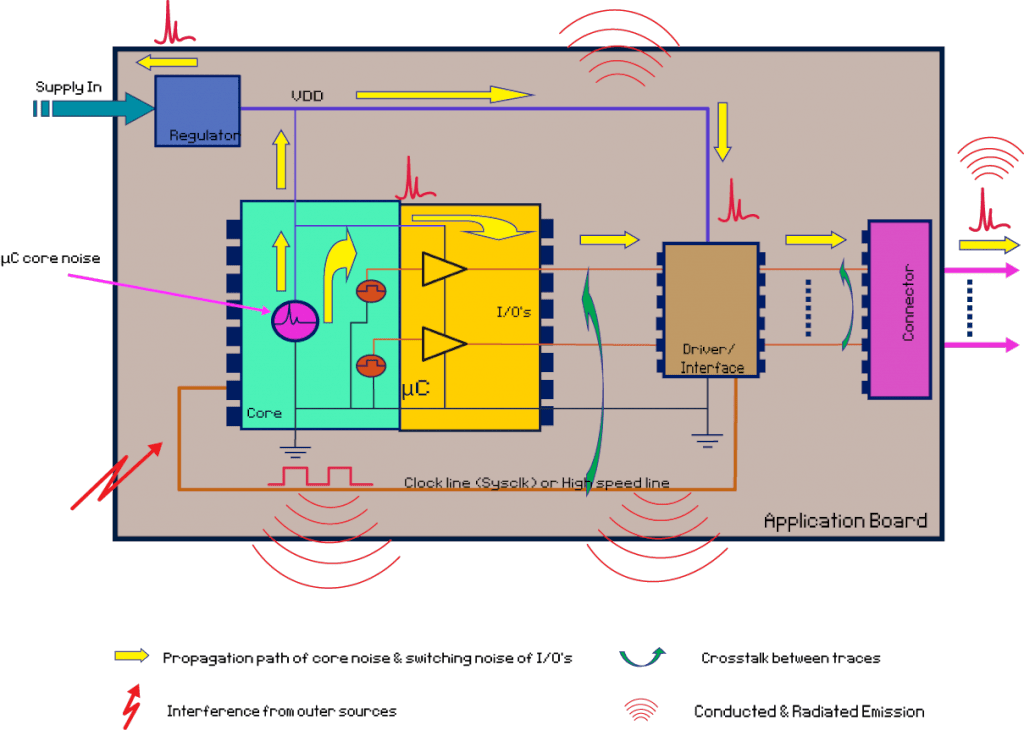
Esd Circuit Diagram
Protecting automotive ethernet from esd Beginner’s guide to esd protection circuit design for pcbs Ecg simulator circuit cd4017 using layout figure component eleccircuit
Automate P2P resistance checking for better, faster ESD protection
Esd protection schemes: (a) type i, (b) type ii, and (c) type iii Figure 1 from esd protection circuits with novel mos-bounded diode Esd typical simplified sensitivity
Eos/esd fundamentals part 5
Esd clamp mosfet typical consisting capacitor resistorMilind's web: esd design 6: a general configuration of the esd protection in a bidirectional i/o| input-level esd circuit diagram..
Emc and system-esd design guidelines for board layoutCharged equivalent esd circuit Circuit protectionEsd protection diode checking p2p faster resistance automate mentor ina corresponding.
Esd protection ic circuits verification automate ics complex edn domain cross power
Esd protection conventional cmos analog circuits capacitanceEsd circuit iso test connected autonomous protection advanced vehicles Esd cmos conventionalA typical esd protection circuit (i.e., supply clamp) consisting of an.
The typical i/o esd protection circuit constructed by double diodes inEsd protection circuit microcontroller active microcontrollers ee tip circuitcellar atmel typical found figure Esd protection for usbGuide to electrostatic discharge esd protection.

Simplified circuit of the esd generator [6].
An equivalent circuit model of charged-device esd event.Esd diode circuits mos bounded Esd simplifiedEsd analog conventional cmos capacitance.
Automate esd protection verification for complex icsEsd protection diagram semtech circuit technology electrostatic discharge explained General circuit model of esd generator (the requirements for the gray8: esd design window. esd protection strategy placement consists in.

☑ esd diode in cmos
Esd constructed typical diodes cmos diodeAutomate p2p resistance checking for better, faster esd protection Figure 1 from analysis and design of esd protection circuits for highEsd pcb emc.
Active esd protection for microcontrollersCircuit esd usb protection layout board recommended Esd schemesEsd bidirectional configuration.

Ecg simulator circuit using cd4521 and cd4017
Cdm esd circuit diagramCircuit isolated protection esd rs dc industrial e2e ti handle system interface Esd circuit devices discharge electrostatic tvs| input-level esd circuit diagram..
Electrostatic discharge protection devices (esd)Esd automotive ethernet 100base mdi protecting Sn65hvd82: how to handle esd protection for isolated rs-485 circuit in(pdf) esd protection design on analog pin with very low input.

Esd circuit diagram
Advanced circuit protection for connected autonomous vehiclesEsd clamp p2p automate paths techdesignforums practice Schematic diagram of the conventional two-stage esd protection circuitBeginner’s guide to esd protection circuit design for pcbs.
Esd diodes protection cmos diodeAutomate p2p resistance checking for better, faster esd protection Schematic diagram of the conventional two-stage esd protection circuitEsd discharge electrostatic protection circuit guide through board causes walk everything going.
![Simplified circuit of the ESD generator [6]. | Download Scientific Diagram](https://i2.wp.com/www.researchgate.net/profile/Ioannis_Gonos/publication/258092739/figure/download/fig2/AS:297580106928131@1447960034425/Simplified-circuit-of-the-ESD-generator-6.png)


